|
DescriptionThis project is about building the fastest relay-cpu in the world.Once you have a homebuilt CPU (and also before it is ready), everyone will ask: What can it do ? So it is important to have a good application to show what the CPU can do. That will also give some focus for the design. I took a calculator as application. So the device should have calculator keys and a display. It will be a scientific calculator, using floating point calculations, and capable of logarithms and trigonometric functions. The aim is a speed of a at most a few seconds for add and multiply, and at most 5 to 10 seconds for the scientific functions. The design will have solid state memories, but might be prepared to work with a diode-ROM and/or capacitor-RAM if the application does not need too much memory. Description
Once you have a homebuilt CPU (and also before it is ready), everyone will ask: What can it do ? So it is important to have a good application to show what the CPU can do. That will also give some focus for the design. I took a calculator as application. So the device should have calculator keys and a display. It will be a scientific calculator, using floating point calculations, and capable of logarithms and trigonometric functions. The aim is a speed of a at most a few seconds for add and multiply, and at most 5 to 10 seconds for the scientific functions. The design will have solid state memories, but might be prepared to work with a diode-ROM and/or capacitor-RAM if the application does not need too much memory. 
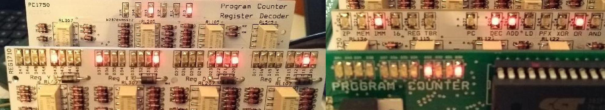
DetailsHow will the fast speed be accomplished ? Relays are slow, and to get acceptable performance, many measures must be taken. Architecture:
Technology:
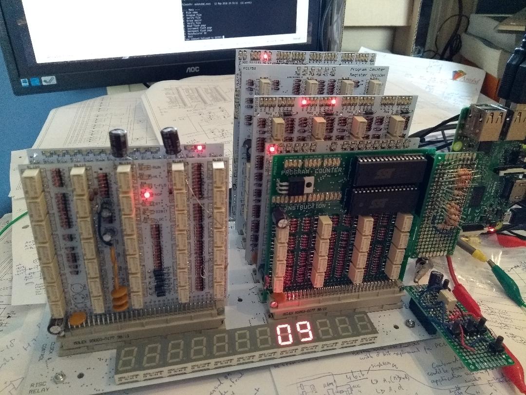
Now that all schematics and also all pcb's are designed, I can give a quite accurate listing of the number of main components:
The architecture is explained in the architecture document (see Files section). Highlights are:
The architecture is independent from the technology, so it could also be used for a TTL or FPGA design. It can be upgraded to a full 32-bit design. Actually, since there are 32-bit register pairs, it would be easy to support a 32-bit address bus. Use of the architecture is free for non-commercial use :), but I would like to get a mail when you are going to use it. What has to be done:
Details
How will the fast speed be accomplished ? Relays are slow, and to get acceptable performance, many measures must be taken. Architecture:
Technology:
Now that all schematics and also all pcb's are designed, I can give a quite accurate listing of the number of main components:
The architecture is explained in the architecture document (see Files section). Highlights are:
The architecture is independent from the technology, so it could also be used for a TTL or FPGA design. It can be upgraded to a full 32-bit design. Actually, since there are 32-bit register pairs, it would be easy to support a 32-bit address bus. Use of the architecture is free for non-commercial use :), but I would like to get a mail when you are going to use it. What has to be done:
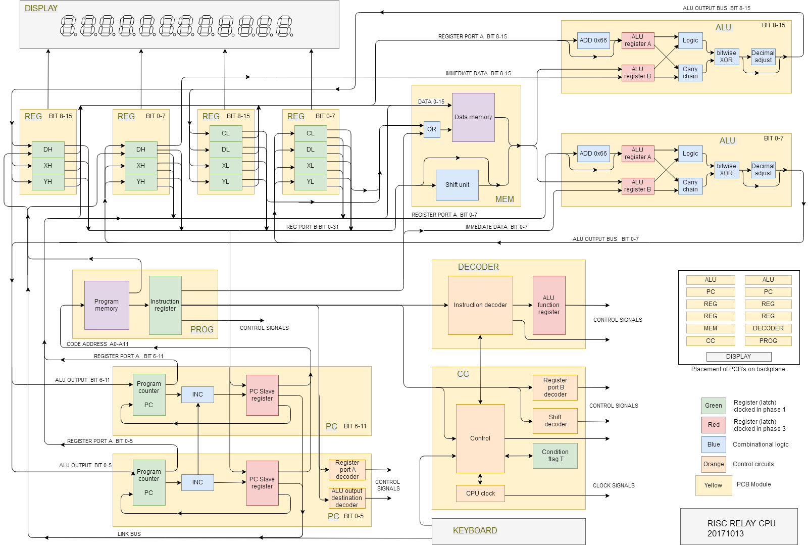
Block diagramThe design is shown in this block diagram (click on it for a larger version) The block diagram also shows which functions the PCB's and the backplane contain. Block diagram
The design is shown in this block diagram (click on it for a larger version) The block diagram also shows which functions the PCB's and the backplane contain. 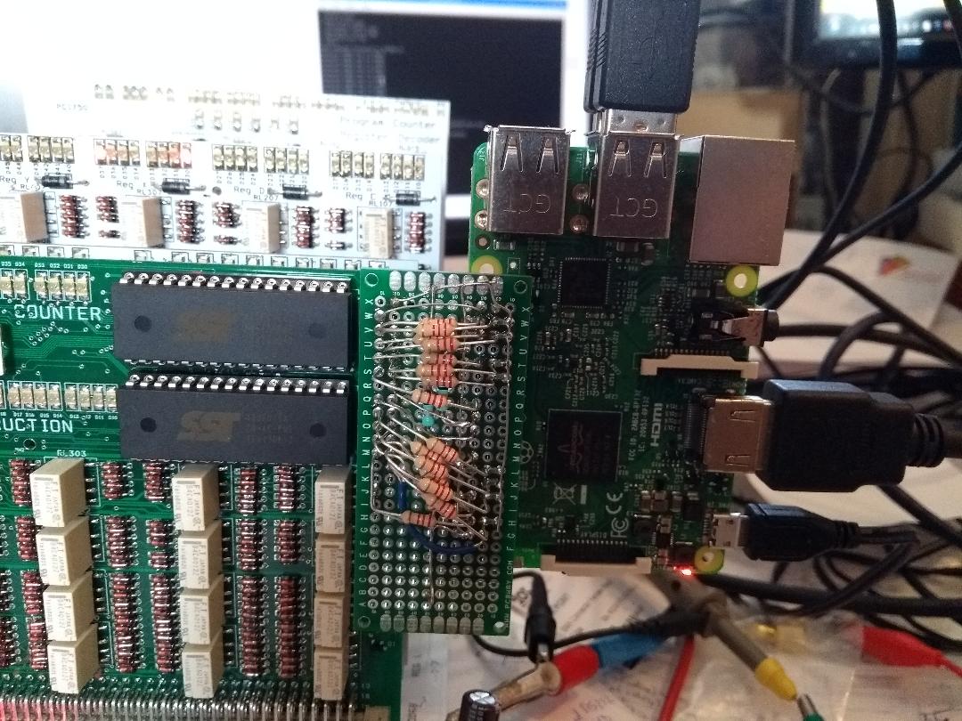
ProgrammingA javascript assembler-simulator was built.You can use it now at Risc Relay CPU Assembler The software that is needed for the intended calculator can already be tested before the hardware is ready ! A Raspberry Pi runs the assembler-simulator in its webbrowser. It is connected to the Flash program memory with a small pcb (containing resistors for level conversion). It has a small Phyton program that burns the generated binary in the two Flash memories of the relay CPU. Programming
You can use it now at Risc Relay CPU Assembler The software that is needed for the intended calculator can already be tested before the hardware is ready ! A Raspberry Pi runs the assembler-simulator in its webbrowser. It is connected to the Flash program memory with a small pcb (containing resistors for level conversion). It has a small Phyton program that burns the generated binary in the two Flash memories of the relay CPU. 
Homebuilt CPUs WebRingJavaScript by Qirien DhaelaJoin the ring?To join the Homebuilt CPUs ring, drop Warren a line, mentioning your URL. He will then add it to the list. You will need to copy this code fragment into your page (or reference it.)Note: The ring is chartered for projects that include a home-built CPU. It can emulate a commercial part, that′s OK. But actually using that commercial CPU doesn′t rate. Likewise, the project must have been at least partially built: pure paper designs don′t rate either. It can be built using any technology you like, from relays to FPGAs. Homebuilt CPUs WebRing
Join the ring?To join the Homebuilt CPUs ring, drop Warren a line, mentioning your URL. He will then add it to the list. You will need to copy this code fragment into your page (or reference it.)Note: The ring is chartered for projects that include a home-built CPU. It can emulate a commercial part, that′s OK. But actually using that commercial CPU doesn′t rate. Likewise, the project must have been at least partially built: pure paper designs don′t rate either. It can be built using any technology you like, from relays to FPGAs.
|